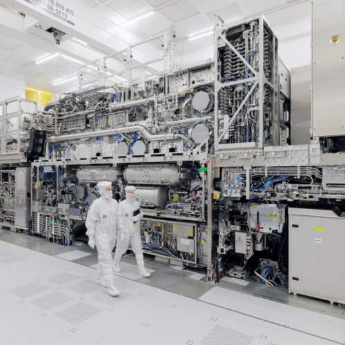
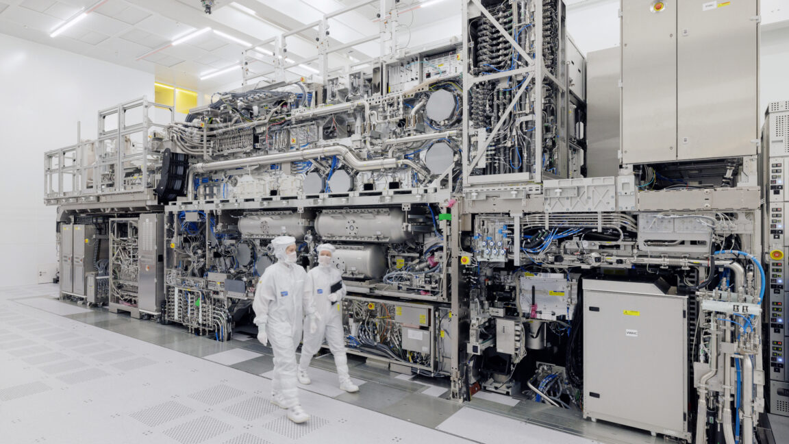
Leading chipmakers Samsung Electronics and Taiwan Semiconductor Manufacturing Co. announced plans to adopt ASML’s latest chipmaking machines in the next several years—and they also joined Intel in agreeing to a crucial technology change that could boost chip production on the new machines by 40 percent.
This signifies the semiconductor industry’s broader embrace of high NA EUV photolithography technology that can cost up to $400 million per machine and is only provided by the Dutch technology company ASML, Bloomberg reports. The technology would allow chip designers to implement even smaller features in potentially more powerful and efficient next-generation chips produced for AI data centers and consumer electronics such as smartphones, tablets, and laptops.
ASML’s EUV (extreme ultraviolet) lithography machines enable chipmakers to use powerful laser light to imprint patterns in silicon wafers, layer by layer, and gradually form the computer circuitry that makes silicon chips work. Compared to older deep ultraviolet lithography, EUV technology harnesses a more powerful source of light with a shorter wavelength to create even smaller features on silicon wafers.
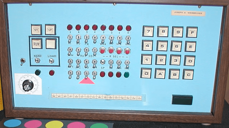
If you were interested in computers in the early 1970s, you struggled to get time on real computers since owning your own was all but impossible. In the middle of the decade, though, you could get a few computers: the Mark VIII, the Altair, the Apple I, and several others. Those were still pretty expensive, though. But in late 1976, an article in Popular Electronics said you could build a “powerful, expandable” computer for $80. The article in question was by [Joseph Weisbecker], who, unknown to most of us at the time, was actually the RCA employee behind the CPU — an RCA 1802. [Tech Time Traveler] takes a close look at the spunky little computer’s history in the video you can see below.
The 1802 was actually the second generation of the CPU, but the first that was all-in-one chip. [Weisbecker] started building the CPU as a personal project. He’d been a hacker even in high school, building relay-based tic-tac-toe games, among other things.
The first incarnation in his lab was “Fred,” with 100 TTL chips, and his idea was to have the computer be at least partially used as a video game — an interesting point, with Pong being very popular at the time.
The video covers a lot of history, but from a hacker’s point of view, the CPU was both amazing and limited. In a day when the 8080 and Z80 were kings, the 1802 had built-in DMA. This allowed a cheap companion video display that simply read bytes from memory and pushed them out to a TV.
Another neat feature was that the device had 16-bit registers and, even more interesting, 16 of them. On the one hand, any register could be, for example, the program counter or a memory index register. But on the other hand, there was no direct stack for doing calls and returns. The idea was that you’d use different registers for different subroutines, which was fine and efficient for very simple programs but not for the general case. One thing all 1802 programmers knew about was SCRT, the “standard call return technique” routines in the 1802 manual. But, as you might expect, this made calls and returns expensive.
There’s more that you’ll see in the video. People still build 1802-based computers and, of course, there are plenty of simulators, including ours. One thing you’ll notice is that the instruction set is very regular. Even if you didn’t know, you might guess that one guy designed the architecture.
Say "Hey Sonos," and your Lutron Caséta lights, shades, and music now respond instantly, no app, no remote, just a voice command through your existing Sonos speaker.

 Login
Login