❌

Reading view

There are new articles available, click to refresh the page.

Big Infinity Mirror Clock Invites You To Gaze Deeply
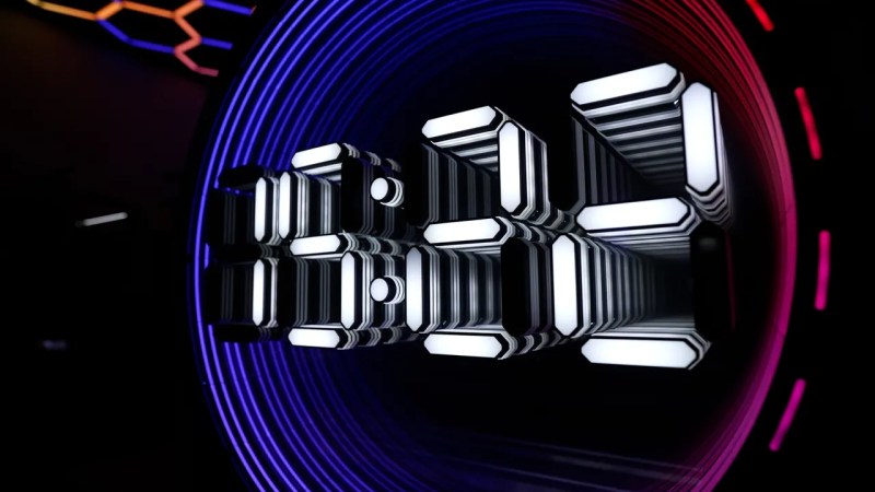
[Andy Huot] has a fantastic-looking infinity mirror digital clock that really raises the bar. It uses high quality components, smart use of RGB LED animations, and a clever β€œstacked diffuser” vertical design to the 7-segment display elements that really enhances the infinity mirror effect. It needs to be seen in action, so check it out.

The end result is expressly portal-like, with the smooth animations of the LEDs really playing into the effect. The size helps, too. It’s 24 inches in diameter, giving it considerable presence.
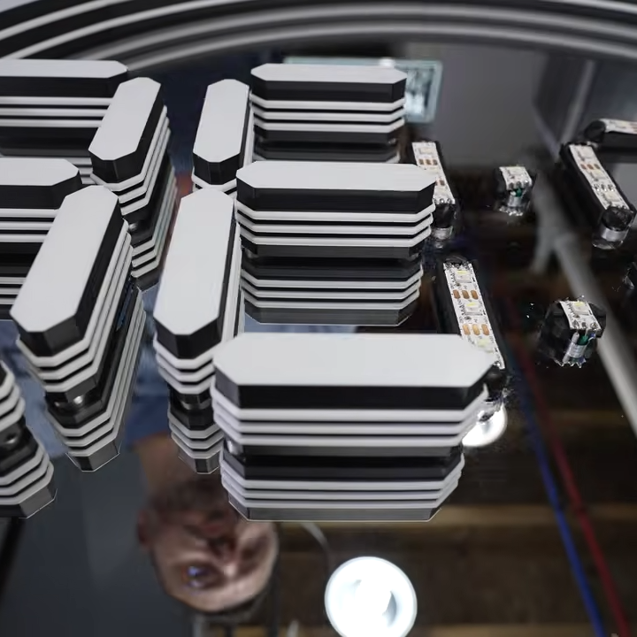
The stacked diffuser design for each display element really enhances the effect.

A basic infinity mirror design consists of lit elements sandwiched between a reflective back surface and a partially-reflective, partially-transmissive top cover. That same basic principle is used here, but with great care given to ensure nothing so much as a fingerprint spoils the illusion. For example, the top cover is a disk of acrylic with a 90% reflective film affixed to the inside surface. That’s easy enough to DIY with some car tint, but [Andy] found that for the very best results it was worth having high-quality film professionally applied.

We like the use of 3D-printed custom jigs for soldering the segments of RGB LED strips, and holding the pre-measured wires in place with some putty is a great way to keep them in place while working. In case you’re wondering, the mirrored acrylic making up the back wall has holes in it for mounting each segment’s LED strip in a holder, and running the wires to the rear.

The video (embedded below) documents every step of the assembly, and it’s a serious build. While the design files for the 3D-printed parts are not free, there’s certainly enough detail for an enterprising hacker to replicate the design in their own way.
Custom AMOLED Wearable Makes Great Icebreaker

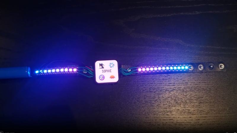
Nifty little AMOLED screens are easy to get nowadays, and [Sophie D] demonstrates they are both thin and light enough to be worn with OpenChoker, a design for a choker necklace that was a hit at DEF CON.

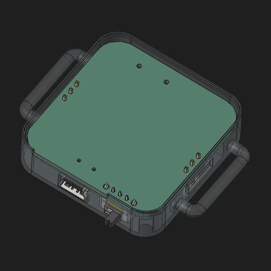
The choker consists of an AMOLED touchscreen flanked by short RGB LED strips. Behind the display is the PCB which contains an RP2350 and micro SD card slot for external storage, and at the rear of the choker is an 18650 cell to power it all. The display plays an eye-catching animation that gets generated on the fly while the LEDs sparkle away.

[Sophie] shares a number of interesting takeaways from designing and building this device. One is that the bulk of the PCB design work was interfacing to the display, since no existing footprint or reference design could be found. So if you find yourself with a Hello Lighting HL020E21-02 2.14β€³ touchscreen display you’re hankering to use in your own project, do yourself a favor and check out [Sophie]’s board design instead of starting from scratch.

Battery life was more than enough for a device like this. A single 18650 cell powered the choker effortlessly for a 16-hour stretch and still the cell measured a robust 3.7 V. While a light-up choker used indoors isn’t a great candidate for wearable solar power, it’s encouraging that there’s no need for a tethered battery pack.

Another tip to consider relates to the screen’s touch sensitivity. In short, the capacitive touch screen responded perfectly when plugged into a development computer, but when mounted and isolated on the choker it responded so poorly as to be useless. It didn’t keep the rest of the choker from doing its job, but it might be worth keeping in mind as something to watch out for with a device like this.

There’s one final mystery [Sophie] ran into: with only one day to spare, glue used to affix some wires ended up melting away the wire insulation, revealing bare copper. We’re not sure what happened there, but if nothing else it’s a reminder that Murphy’s Law is always ready to strike when one is on a deadline.

Building An Energy-Harvesting Business Card

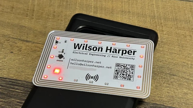
The hope is always that a good business card will leave a good impression. For those in the electronics field, they also serve as an opportunity to showcase creative design skills. [Wilson Harper] demonstrates that ably with a rather nifty energy-harvesting build.

The card is based around a thin PCB in the typical business card size. It’s populated by 21 Charlieplexed LEDs, a small microcontroller, and some supporting components. Now, this is normally where you might expect the device to be powered by a small coin cell, maybe deftly integrated into the PCB thickness itself to make the card less cumbersome. But noβ€”[Wilson] went a different route. The thing is that in 2026, most of us are carrying phones with NFC readers built in. Thus, the card was built to harvest this source of energy with a PCB trace antenna, designed with the aid of STM’s antenna inductance tools and an LLM script lobbed into KiCad. All one needs to do is to pop the card on the back of a phone and the LEDs animate joyfully.

Design files are on Github for the curious. You might also like to check out some of the fancy business cards we’ve featured in the past. Of course, if you’re working on just such a project yourself, you’re more than welcome to send it in to the tipsline!

Making LEDs in the Home Fab

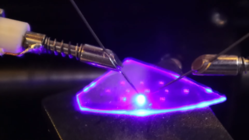
An irregular shard of a crystal wafer is set on a table, with two wire probes contacting it. Between the probes, a bright blue-purple light glows, illuminating the rest of the wafer.

Impressive as it most certainly is when an amateur fabricates a semiconductor, most of the projects we’ve seen are more demonstrations than workable chips. [Dr. Semiconductor], however, is going much further with his fabrication process, and is already working on a method to bond chips to printed circuit boards. It’s difficult to align a PCB with the pads on the underside of an opaque silicon wafer, however, so as a trial run he’s made and bonded some transparent LED chips.

The starting material for these chips is a gallium nitride (GaN) LED epiwafer, a stacked structure of n-doped GaN, an indium gallium nitride quantum well layer, and p-doped GaN grown on a sapphire substrate. When current passes through the structure, electrons from the n-doped layer and holes from the p-type layer recombine in the quantum well layer, emitting blue light. To make a functional LED from this, [Dr. Semiconductor] needed to make electrical contacts to both the n-type and p-type layers. Making the n-type contact required cutting through the p-type and quantum well layers.

This would normally be done with reactive ion etching in chlorine, but [Dr. Semiconductor] came up with a new process: a 355-nm ultraviolet etching laser causes GaN to break down into gallium and nitrogen, with the resulting cut being cleaned up by a potassium hydroxide etch. To deposit the contacts themselves, [Dr. Semiconductor] formed a photoresist mask, deposited metal (nickel, silver, and titanium) in a sputtering chamber, and used a developer solution to dissolve the mask and lift off the unwanted metal regions.

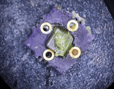
A square, purple PCB is shown under a microscope. The PCB has four vias surrounding a transparent chip, which has a blob of translucent yellow material on top of it.
The LED after bonding and phosphor application.

When [Dr. Semiconductor] applied current between the two contacts, the LED glowed bright blue. The next step was to mount it to a PCB; to do so, he first sliced the wafer into individual LED chips with the ultraviolet laser. He then electroplated indium bumps onto a printed circuit board, positioned the chip above these bumps, added some rosin flux, and melted the indium bumps. This soldered the chip to the board and let the board power the LED.

Like most commercial LEDs, these were blue; most LED assemblies additionally include a phosphor layer which absorbs blue light and emits another color. To create a white LED, for example, [Dr. Semiconductor] mixed cerium-doped yttrium aluminium garnet phosphor powder with clear silicone and spread it over the LED. This absorbs some of the blue light and emits yellow light, and the resulting mixture of blue and yellow light looks white to human eyes.

We’ve previously covered some of the history of LEDs and the phosphors which make them useful. This seems to be the first inorganic LED we’ve seen, but we’ve also seen a few homemade OLEDs.

Thanks to [SpuriousIndices] for the tip!

Foldable OLED Displays and the Bane of Dust

Much like Apple’s once vaunted super-slim butterfly keyboard, today’s range of portable devices featuring flexible OLED displays – which can fold said display into a much smaller form factor – are a marvel of engineering.

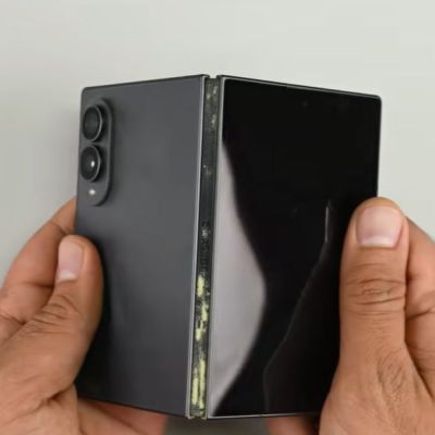
The foldable phone after a dusty encounter. (Credit: iFixit, YouTube)

Unfortunately engineering can only do so much against fundamental flaws. In the case of both these flexible OLEDs and butterfly keyboards the main issue is that of dust intrusion, with a recent teardown by [iFixit] going over the reasons for this.

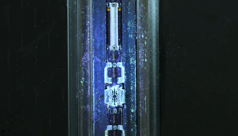
As test subject we got a Galaxy Z Fold 8, as an example of a modern-day foldable smartphone-tablet hybrid. This phone has an IP48 rating, meaning that it’s water-resistant, but not dust-resistant for particles smaller than 1 mm. To test this, [iFixit] used UV-reactive dust particles, making sure that they got literally everywhere inside the phone’s hinge mechanism.

After this treatment, trying to fold the phone caused the hinge mechanism to make absolutely horrific crunching noises, confirming that it’s reached dust-under-butterfly-keycap levels of unusable. During the subsequent teardown a quick pass with the UV lamp showed that not much of the dust had penetrated into the two halves of the device at least, but the hinge mechanism wasn’t as lucky.

Getting to the hinge is sadly rather destructive, as it involves removing the flexible OLED. Once the hinge was exposed and subjected to UV light the spectacle was something to marvel at, as can be seen in the above screenshot. With the dust caking literally every part of the mechanism, it was little wonder that the hinge had ceased to work.

Although this was obviously an extreme case of dust exposure, and the average flexible OLED screen’s hinge won’t see nearly as much dust, one can’t help but feel slightly disconcerted at that crunching noise, knowing that it’s just one big dust exposure away.

❌